
We Think Laser, Lasers for Industry, the Mark of Excellence; the Ongoing Miniaturization of Electronics, Semiconductor and Medical Devices Opens Up Unique Possibilities for Lasers. Where Traditional Material Processes Reach their Limits, Lasers Open Up new Possibilities Due to Excellent Focussing and a Small Heat Affected Zone. Whether Metal, Plastics, Glass, Semiconductor Parts, Ceramics or Wood – Almost all Materials can be Marked with a Laser, with Speeds Up to 1,000 Characters Per Second. Today, Semiconductor Industry, Machine Parts ...
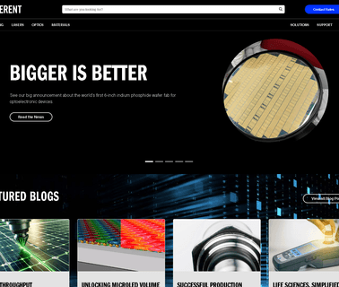
Iii V Multi Layer Epitaxial Wafer Production Services. Public Access to Cleanrooms & Process Tools. the Center for High Technology Materials is a 60,000 Square Foot Research Facility at the University of new Mexico. We have two Cleanrooms Open to the Public which offer a full Suite of Semiconductor Process Tools for Fabricating State Of The Art Iii V, Silicon, Glass, Heterogeneous Materials and Devices for Photonic, Laser, Optical Communication; Applications. as a State Funded Faciliity, we, Optics Equipment, Photonics ...
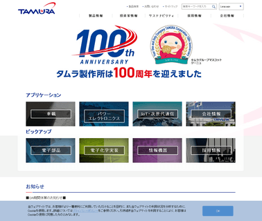
Single Crystal Gallium Oxide Substrates and new Phosphor for Blue Laser Applications; Gallium Oxide (Ga2O3) Crystal is a Promising Material that Tamura has Put into Practical use for the first Time in the World. the new Semiconductor Crystal is Transparent in the Ultraviolet Visible Region and Electrically Conductive. Using this Crystal, Ultra High Power Gan Leds and Ultra High Voltage Power Devices are Realized. In Addition, we Release a new Phosphor for Blue Laser Applications, Laser Projector, Media Broadcasting ...